What’s Happening at Xinyx

Get the latest scoop on our company happenings. Explore articles, event highlights, and updates that showcase our impact in the microelectronics space.

Blogs & Insights

Curious minds welcome. Our monthly blogs offer fresh takes on IC design, engineering culture, and innovations that matter.

Chip Designer
The modern world runs on silicon chips, but few outside the semiconductor industry truly understand the microscopic marathon required to create them. At the heart of this process are two intertwined, yet vastly different, disciplines: IC Design (the Front-End) and IC Layout (the Back-End, or Physical Design). This Xpert Insights Trivia piece explores the essential distinction: IC Design is the architectural, logical, and abstract phase where engineers define what the chip does using code and models. It culminates in the Gate-Level Netlist, a massive list of digital instructions. IC Layout, conversely, is the physical, geometric, and concrete phase where engineers transform that netlist into actual shapes on the silicon wafer. It involves complex challenges like minimizing wire length, distributing power without voltage drop, and routing billions of connections perfectly—all while adhering to the unforgiving laws of physics and the foundry's manufacturing rules. The Layout team is responsible for the critical Design Closure and delivering the final GDSII file—the chip's literal blueprint for fabrication. Understanding this division—from the logical world of RTL to the physical world of parasitics and DRC—is the key to successful, high-performance silicon development.
Unlocked 2025 Innovators

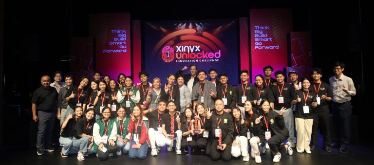
UNLOCKED 2025: THINK BIG, BUILD SMART, GO FORWARD Muntinlupa City, October 17, 2025 – Now in its third year, Xinyx Unlocked stands as the flagship talent development initiative of Xinyx Design, serving as a platform to empower the next generation of Filipino innovators from across the country. Promoting inclusivity in innovation, the event brings together […]

The modern world runs on silicon chips, but few outside the semiconductor industry truly understand the microscopic marathon required to create them. At the heart of this process are two intertwined, yet vastly different, disciplines: IC Design (the Front-End) and IC Layout (the Back-End, or Physical Design). This Xpert Insights Trivia piece explores the essential distinction: IC Design is the architectural, logical, and abstract phase where engineers define what the chip does using code and models. It culminates in the Gate-Level Netlist, a massive list of digital instructions. IC Layout, conversely, is the physical, geometric, and concrete phase where engineers transform that netlist into actual shapes on the silicon wafer. It involves complex challenges like minimizing wire length, distributing power without voltage drop, and routing billions of connections perfectly—all while adhering to the unforgiving laws of physics and the foundry's manufacturing rules. The Layout team is responsible for the critical Design Closure and delivering the final GDSII file—the chip's literal blueprint for fabrication. Understanding this division—from the logical world of RTL to the physical world of parasitics and DRC—is the key to successful, high-performance silicon development.

Insights

Stay ahead with expert perspectives, industry trends, and deep dives into the world of IC design and everything tech!

Subscribe to our Newsletter!

Be updated with our news about IC Design and Microelectronics!