
Unpacking the IC Digital Design Flow: The Essential Difference Between Front-end Design and Back-end Design in VLSI
The tiny chips powering everything from our space-faring satellites to the smartphones in our pockets are the unsung heroes of the digital age. But before an Integrated Circuit (IC) can be manufactured, it must survive a highly complex, multi-stage process known as the IC Design Flow.
Within this flow, two distinct disciplines stand out, representing the fundamental split between abstract logic and physical reality: IC Front-End Design and IC Back-End Design. In most of the industry, the term “Digital Design Engineer” is used for the Front-End Design specialists while “Physical Design Engineer” is the term used for Back-End. It is important that Digital Design Engineer is not misconstrued as encompassing the whole Digital Design Flow; rather it refers specifically to Front-End.
Understanding the precise difference between these two roles is critical for anyone in the Very Large Scale Integration (VLSI) industry, whether you’re an aspiring engineer, a product manager defining timelines, or a partner seeking specialized silicon expertise.
In this deep dive for Xpert Insights, we illuminate the contrasting challenges, tools, and objectives of the Front-End and Back-End engineers and show why success in modern electronics hinges on seamless collaboration between them.
Part I: The Front-End Engineer– Defining the Brain
The Role of the Digital Design Engineer: From Concept to Verified Logic
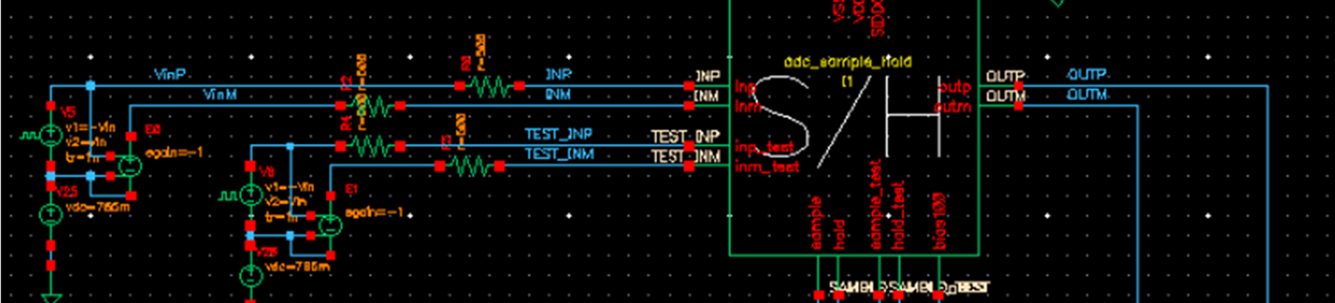
The Front-End Design phase is the conceptual stage. It is purely abstract and logical, focused on defining what the chip will do and how its components will interact mathematically. The Front-End engineer is the system architect—the person who translates high-level specifications (like “must process 4K video at 60fps” or “must consume less than 1mW of power”) into digital logic.
Key Activities of the Front-End Engineer:
- System Architecture and Specification: Defining the block diagram and macro-level partitioning of the chip. This determines the major components (CPU cores, memory, I/O ports, etc.) and their communication paths.
- RTL Coding (Register-Transfer Level): Using Hardware Description Languages (HDLs) like Verilog or VHDL to describe the circuit’s functionality and logic gates. This code is the abstract instruction set for the chip.
- Functional Verification: This is the most time-consuming and critical task. The designer creates test benches and simulations to prove that the RTL code performs exactly as required, across all possible operating conditions and corner cases. They ensure the logic is flawless before it touches the physical world.
- Logic Synthesis: Using automated Electronic Design Automation (EDA) tools, the designer translates the HDL code into a Gate-Level Netlist. This netlist is a giant list of standard cells (pre-designed NAND, NOR, and Flip-Flop gates) and their interconnections. It remains a logical description, but now it is tied to specific standard cell characteristics from the foundry’s library.
In essence, the Front-End Engineer focuses on the chip’s intelligence, functionality, and performance targets, working almost entirely in the digital and logical domain.
Part II: The Back End Engineer – Building the Physical City
The Role of the Physical Design Engineer: From Netlist to GDSII Tape-Out
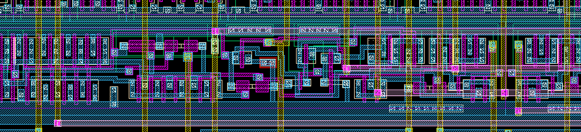
The Back-End Design phase, also known as Physical Design, is the implementation stage. It is purely concrete and physical, focused on translating the abstract logic (the netlist) into actual geometric shapes on the silicon substrate. The Physical Designer, or Back-End specialist, is the city planner—the person who ensures the design can be manufactured and operates correctly under real-world physical laws.
The work starts where the designer stops: with the gate-level netlist.
Key Activities of the Back End Engineer:
- Floorplanning: Deciding the physical dimensions of the chip and the placement of large functional blocks (IP cores, memory blocks, analog modules). This sets the stage for the rest of the layout and is crucial for meeting timing and power constraints.
- Power Planning: Designing and routing the dedicated power and ground metal grids across the entire chip. At nanometer scales, voltage drop (IR Drop) and signal noise become major issues if the power network is not meticulously planned.
- Placement: Arranging the hundreds of thousands or even billions of standard cells (gates) defined in the netlist into the core area. Placement must be optimized to minimize the length of interconnecting wires and prevent congestion.
- Clock Tree Synthesis (CTS): Building a network of buffers that distributes the chip’s master clock signal to every single flip-flop with minimal skew (timing variation). The clock is the heartbeat of the chip, and precise CTS is vital for synchronous design.
- Routing: Connecting all the placed components (gates and blocks) using multiple layers of metal interconnects. This is governed by extremely strict Design Rule Check (DRC) rules imposed by the foundry (minimum width, minimum spacing, etc.).
- Physical Verification and Signoff: This is the final gate. The layout engineer performs exhaustive checks:
- DRC (Design Rule Check): Ensures no manufacturing rules are violated.
- LVS (Layout Versus Schematic): Guarantees the physical layout perfectly matches the original logical netlist.
- Static Timing Analysis (STA): The final, post-layout timing check. This accounts for the actual resistance and capacitance (parasitics) introduced by the real metal wires, ensuring the chip meets its speed requirements in silicon.
The Physical Design Engineer focuses on the chip’s manufacturability, timing closure, power distribution, and final physical integrity, working in the geometrical and electromagnetic domain.
The Crucial Interdependency: Where the Domains Collide
The separation between Front-End and Back-End is essential for dividing complexity, but they are intrinsically linked. The quality of the Front-End design directly impacts the difficulty of the Back-End layout, and vice versa. Digital Design engineers rely on Physical Design Engineers for the extraction of their physical designs to validate the performance of their logical abstractions, while Physical Design Engineers rely on a well-structured front-end design to create a feasible physical layout. This constant hand-off illustrates the interdependence of each discipline.
The Feedback Loop of Convergence
A poorly planned Front-End design might lead to Routing Congestion (too many wires trying to occupy the same small area) or Timing Violations (signals arriving too late due to long, resistive wires). When this happens, the Physical Design team must send the design back, forcing the Front-End team to restructure their logic—an expensive iteration called Design Closure.
Conversely, the Physical Design team’s ability to create a clean, efficient physical map directly determines the final Power, Performance, and Area (PPA) metrics of the chip. In advanced technology nodes (like 7nm or 5nm), physical effects dominate, and this influence becomes more evident during post-simulations. A design that passes all pre-layout simulations may fail to meet its targets once extractions from the physical design are included. In other words, a “perfect” Front-End Design can be invalidated by the realities of layout implementation. This forces both to re-evaluate their work whether the issue can be solved by front-end redesign or by restructuring the physical design.
This is why modern VLSI teams demand engineers who possess not only deep expertise in their domain but also an appreciation for the challenges of the other.
Xinyx Design: A Leader in IC Design and Layout
Our team at Xinyx is recognized as a leader in providing comprehensive Integrated Circuit Design and Layout services. We specialize in navigating the most demanding aspects of the VLSI flow, with a particular focus on high-speed Analog/Mixed-Signal (AMS) IC Layout and Advanced Node Digital Physical Design at 7nm, 5nm, and down to the latest technology.
Our engineers possess the rare blend of Front-End architectural knowledge and Back-End physical precision required to ensure rapid Design Closure and deliver final GDSII files that are fully compliant, optimized for PPA, and guaranteed for manufacturability. We provide the expertise that ensures your innovative designs transition flawlessly from concept to market-ready hardware.
Partner with Xinyx, the proven authority in mastering the complexity of modern IC design and physical implementation.
Author

Engr. MJ Malubay
Xinyx Training Supervisor